


|
|
|
|
|
Polycrystalline wafers are made by a casting process in which molten silicon is poured into a mould and allowed to set. Then it is sliced into wafers. As polycrystalline wafers are made by casting they are significantly cheaper to produce, but not as efficient as monocrystalline cells. The lower efficiency is due to imperfections in the crystal structure resulting from the casting process. Almost half the silicon is lost as saw dust in the two processes mentioned above. Amorphous silicon, one of the thin film technologies, is made by depositing silicon onto a glass substrate from a reactive gas such as silane (SiH4). Amorphous silicon is one of a number of thin film technologies. This type of solar cell can be applied as a film to low cost substrates such as glass or plastic. In solar cell production the silicon has dopant atoms introduced to create a p-type and an n-type region and thereby producing a p-n junction.
| This doping
can be done by high temperature diffusion, where the wafers are placed in a
furnace with the dopant introduced as a vapor. There are many other methods of
doping silicon. In the manufacture of some thin film devices the introduction of
dopants can occur during the deposition of the films or layers.
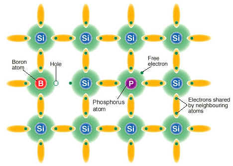
A silicon atom has 4 relatively weakly bound (valence) electrons, which bond to adjacent atoms. Replacing a silicon atom with an atom that has either 3 or 5 valence electrons will therefore produce either a space with no electron (a hole) or one spare electron that can move more freely than the others, this is the basis of doping. p-type doping, the creation of excess holes, is achieved by the incorporation into the silicon of atoms with 3 valence electrons, most often boron and n-type doping, the creation of extra electrons is achieved by incorporating an atom with 5 valence electrons, most often phosphorus. (reference 18) |
|
![]()